Etching Si
Jika kamu sedang mencari Etching Si, maka anda berada di halaman yang tepat. Kami menyediakan aneka Etching Si yang bisa anda pesan online. Silakan hubungi kami via +62811xxxxxxxx, jangan lupa sertakan juka gambar yang diinginkan.
Kami mengirim paket Etching Si melalui berbagai ekspedisi, misalnya JNE, JNT, POS, dll. Kami juga menerima pembayaran via BCA/Mandiri/dll. Pengiriman biasanya tidak sampai seminggu sudah sampai dan kami sertakan pula nomor resi yang bisa digunakan untuk tracking barang secara online.

Tidak hanya Etching Si, anda juga bisa melihat gambar lain seperti Slope Surface, Wet, Deep, Koh, Dry, Resist, Cl2, Zep520a Mask, Plasma, Back, Bosch Plasma, Island Chemical, Circuit Board, Copperplate, Silicon Wafer, Easy Glass, Rembrandt Self Portrait, Colored Glass, Medieval War, Printed Circuit Board, Printmaking Artists, Ferric Chloride, Hard Ground, and Test Print.
Berbagai Contoh Etching Si
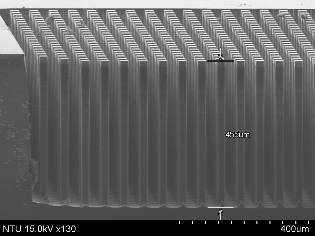
Berikut kami sertakan berbagai contoh gambar untuk Etching Si, silakan save gambar di bawah dengan klik tombol pesan, anda akan kami arahkan pemesanan via WA ke +62811xxxxxxxx.

 0 x 0
0 x 0
wet etching process sio etching sin etching aluminium etching chemical etching youtube


 1379×1039
drie icp rie xef dry silicon isotropic wet chemical acidbase thick thin film etching
 250×187
etchng devices specifications thin film deposition photolithography etching services


.jpg)
.jpg)
Don't forget to bookmark Etching Si using Ctrl + D (PC) or Command + D (macos). If you are using mobile phone, you could also use menu drawer from browser. Whether it's Windows, Mac, iOs or Android, you will be able to download the images using download button.
It seems we can't find what you're looking for.